Demystifying the TPU (Tensor Processing Unit)
For my side quests at Google working on vLLM on TPUs, I had to get up to speed with TPU architecture quickly. This blog post is a crash course on TPUs, where I go down a few rabbit holes to drill some concepts. I think jargon is one of the most frustrating things ever, but unfortunately necessary to read and understand other people’s work. So, as I go along I try to explain every piece of jargon that other introductory guides expect you to magically know already.
What even is a TPU?
Simply put, a TPU is a specialized “thing” built for accelerating AI. It accelerates AI by being able to perform many matrix multiplications very quickly. This is somewhat in contrast to GPUs, which are focused on general purpose acceleration for any tasks.
To explain TPU architecture simply, I think it’s easier to start from a high level overview and then crawl deeper into the individual TensorCore, which is the most important parts to understand compute and bandwidth constraints. I will also introduce some jargon here.
A high level overview - from smallest to biggest unit
TensorCore: The smallest, most important unit people generally will talk about is the TensorCore. This is the actual compute engine, which we will dive into in the next section.
Die (chiplet): One single piece of silicon, with 1 - 2 TCs on it.
Chip: The infamous “chip”. This refers to the die(s) plus the HBM (high bandwidth memory) in one package. This is what people refer to when they say “a single TPU”.
Above this, we get into TPU clustering territory. This is less relevant, but here is the structure.
TensorCore                    the compute engine (MXU, VPU, scalar unit)
└── Die (chiplet)             one piece of silicon, 1-2 TCs
    └── Chip                  die(s) + HBM in one package = "a single TPU"
        └── Tray / Board      ~4 chips on one board, wired together
            └── Host (VM)     CPU machine attached to the tray's chips
                └── Cube      4x4x4 = 64 chips, ~1 rack (16 trays)
                    └── Slice a user-allocated subset of the pod, built from cubes
                        └── Pod       the full set of chips on one ICI network
                            └── Multislice    several slices/pods linked over DCN
The main things to remember however, are TensorCore → Die → Chip.
The important stuff (The Chip)
what is the chip??
I feel its necessary to re-emphasize that the “chip” refers to the die(s) + HBM, and is considered “one TPU”.
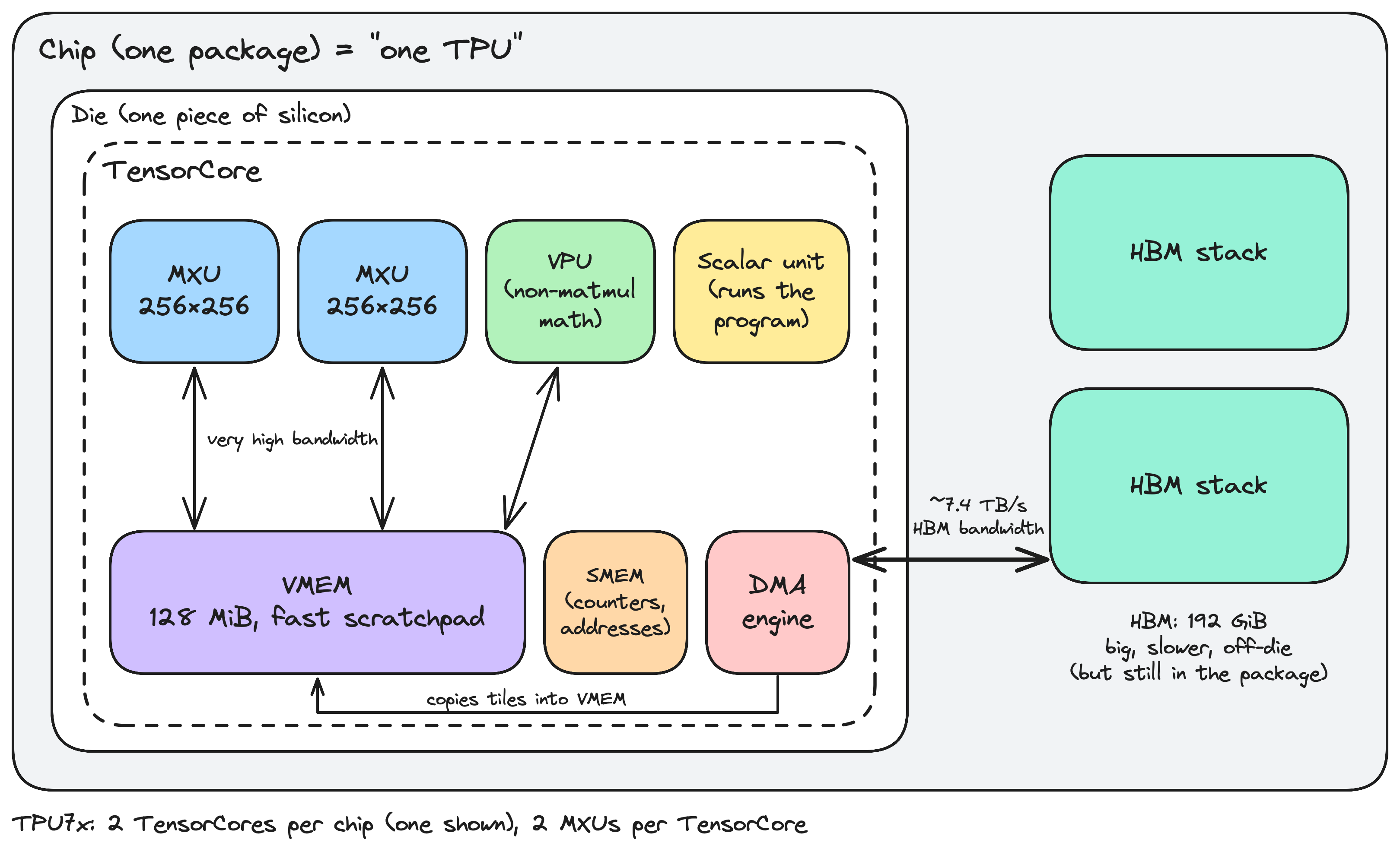
Note: 64 MiB VMEM per TensorCore, 128 MiB per chip.
TensorCore
A Chip will have one or two (depends on generation) “engines”, dubbed TensorCores. These TensorCores have 5 main components (3 are compute units, 2 are memory units). By “unit” I mean “thing”.
There are three core compute units of a TensorCore:
-
The MXU (Matrix Multiply Unit)
The MXU is the core of the TensorCore. Its job, as the name suggests, is to perform Matrix Multiplication (matmuls for short). An interesting thing to note is that it does not perform matmuls with the entire two matrices you are multiplying, which seems like the most obvious approach. The dimensions of the matmuls it performs depends on precision type and generation of TPU.
For example, for on TPU7x, for bf16, it performs one [8,256] @ [256,256] → f32[8,256] matmul every 4 cycles. More on why it doesn’t just do the whole fricking matmul later.
A TensorCore actually has multiple MXUs working in parallel (on TPU7x, each TensorCore has 2 MXUs, and each chip has 2 TensorCores).
-
The VPU (Vector Processing Unit)
This unit performs all the math that isn’t a matmul. It often does elementwise operations. It has a direct link to VMEM, or vector memory.
-
The Scalar Unit (No abbreviation)
The manager of the whole operation. It runs the program itself, and tells the VPU, MXU and DMA engine what to do each cycle. It does almost no heavy math.
what is the DMA engine?
The part of the TensorCore that copies data from one memory to another, mainly between HBM and VMEM, without the compute units having to do the copying themselves.
what is a cycle?
A cycle is one tick of the chip’s internal clock, a signal that pulses billions of times per second to keep every part of the chip in step.
Now, there are also two memory units in a TensorCore:
-
VMEM (Vector Memory)
An on-die scratchpad, that sits very close to the compute units. It is much smaller than HBM (On TPU7x, VMEM = 128 MiB vs. HBM = 192 GiB).
However, it has a much higher bandwidth to the MXU. Data in HBM gets copied into VMEM before MXU can use it.
-
SMEM (Scalar Memory)
On-die. Holds single values the program needs to work. Things includes things like loop counters, addresses, indices, etc.
but wait… this section is called “the Chip”? Isn’t the Chip these 5 things, PLUS the HBM?
Yes.
HBM (High Bandwidth Memory)
The HBM is a big ‘ol chunk of fast memory (when compared to ordinary memory) that stores tensors for use. Although it is on-chip, it is off-die. Which means, in comparison to VMEM and SMEM, it’s slower to retrieve stuff from, because it is physically further away from the compute units.
what is a tensor?
A tensor is just a multi-dimensional array of numbers (a vector is 1D, a matrix is 2D, and so on), and it’s what model weights and activations are stored as.
So, whenever we need tensors for a computation, they are streamed out of HBM through VMEM and into the MXU. Then the result is written from VMEM back to HBM. The thing doing the copying is the DMA Engine.
what is bandwidth?
Bandwidth refers to how many bytes can move between two places per second.
The rate at which data flows from HBM through VMEM into the TensorCore is called the HBM bandwidth.
How a matmul flows through a TensorCore
Now that we know all the different components making up a TPU chip, we can examine how they work together to do speedy matrix multiplication for AI workloads.
Why the MXU works on small tiles
Earlier I mentioned that the MXU doesn’t work on the entire A and B matrices being multiplied (for A @ B). Instead, it works on fixed dimension matmuls.
The MXU is a fixed-size grid of multiply-accumulate circuits (on recent TPUs, 256 x 256 of them). That grid is fixed hardware. It can’t grow to fit the input A and B matrices, so instead we have to shrink the matrices being multiplied. A big matmul gets chopped into small pieces called tiles, and the MXU works through them one after another, adding up the partial results as it goes.
And the matrices in a real model are huge!!! A single weight matrix can be on the order of gigabytes, while VMEM is only 128 MiB. So even if the MXU could swallow the whole thing, there’d be nowhere on-die to load it.
what is a systolic array?
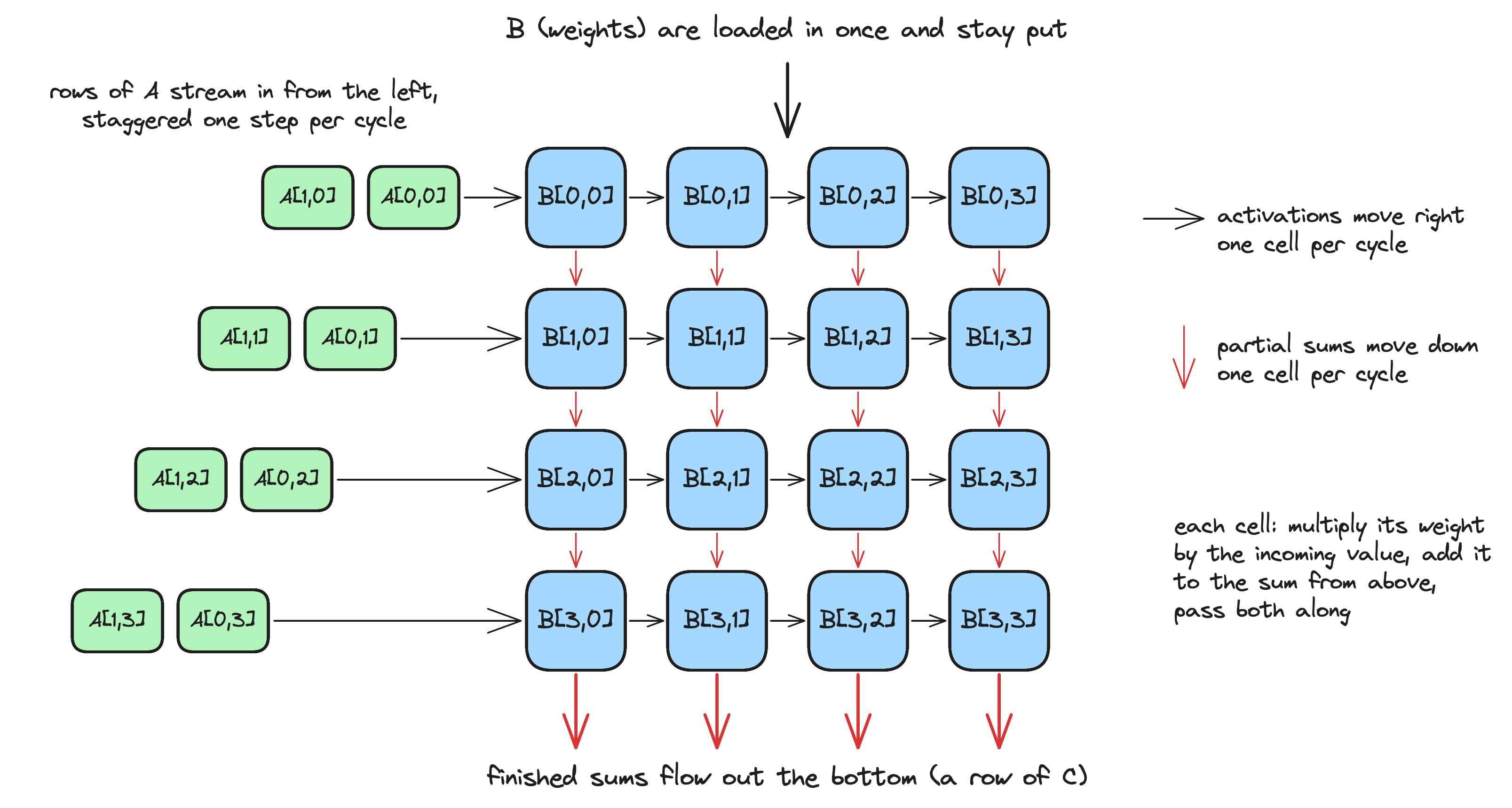
The name for how the MXU is wired. Weights from one matrix get loaded into the grid and sit there, and the other matrix streams through it, with every circuit passing its result to its neighbor on each cycle.
Here’s a small 4×4 version of a systolic array (the real MXU is 256×256):
Why does the tiling approach work?
You can skip over this section if it already makes sense why tiling is used to break down the large matmuls.
The reason this multiply-by-chunks-and-add-them-up approach works comes down to the math behind matrix multiplication. Say we are computing C = A @ B. A column in C only needs a single column of B (plus all of A). Likewise, a row in C only needs a single row of A (plus all of B). Every value in C is just one row of A dotted with one column of B.
That means two things:
- Output columns are independent: if B is too wide for the MXU, we can slice it into column-chunks, multiply each chunk separately, and place the results side by side in C.
- The dot product is a sum, and sums can be split: A dot product over 1,024 numbers is the same as four dot products over 256 numbers each, added together. So if the shared dim. (columns of A and rows of B) is too long for the MXU, we multiply one 256-wide slice at a time and keep a running total.
This was a bit tricky for me to grasp, but just sit down with two small matrices of dims [3, 2] and [2, 3] and do the math by hand, while verifying the above claims.
The tiling loop: HBM → VMEM → MXU → HBM
Let’s walk through a real matmul. Say we want to compute C = A @ B, where:
- A is [16, 512]
- B is [512, 256]
- C is therefore [16, 256]
The MXU on TPU7x, for bf16 can only do an [8, 256] @ [256, 256] matmul at a time. B is too tall, and A is too wide and too tall, so we cut the shared dimension in half and split A’s rows into chunks of 8:
- A becomes four tiles: A₀,₀ and A₀,₁ (the two row-chunks of the first column slice) and A₁,₀ and A₁,₁ (the two row-chunks of the second column slice), each [8, 256]
- B becomes two tiles: B₀ and B₁, each [256, 256]
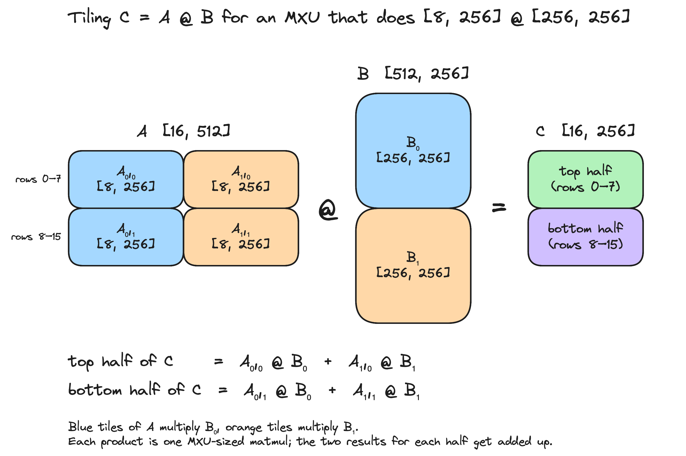
Then the top half of C (rows 0-7) is A₀,₀ @ B₀ + A₁,₀ @ B₁, and the bottom half (rows 8-15) is A₀,₁ @ B₀ + A₁,₁ @ B₁. This is how the hardware computes this:
- The scalar unit tells the DMA engine to copy B₀ and A₀,₀ from HBM into VMEM.
- B₀ gets loaded from VMEM into the MXU, where it sits still for as long as we have chunks of A to stream through it.
- A₀,₀ streams from VMEM through the MXU. The result comes out the other side and lands in VMEM as a running total for the top half of C.
- A₀,₁ is fetched and streams through the same B₀, which hasn’t moved. Its result lands in VMEM as a running total for the bottom half of C.
- Repeat for the next chunk: fetch B₁, A₁,₀ and A₁,₁, load B₁ into the MXU, stream A₁,₀ through and add the result to the top running total, then stream A₁,₁ through and add the result to the bottom running total.
- If there’s any non-matmul math left (an activation function, say), the VPU does it, straight out of VMEM.
- The DMA engine copies the finished C from VMEM back out to HBM.
The scalar unit keeps track of where it is using loop counters and addresses stored in SMEM. Mostly boring stuff.
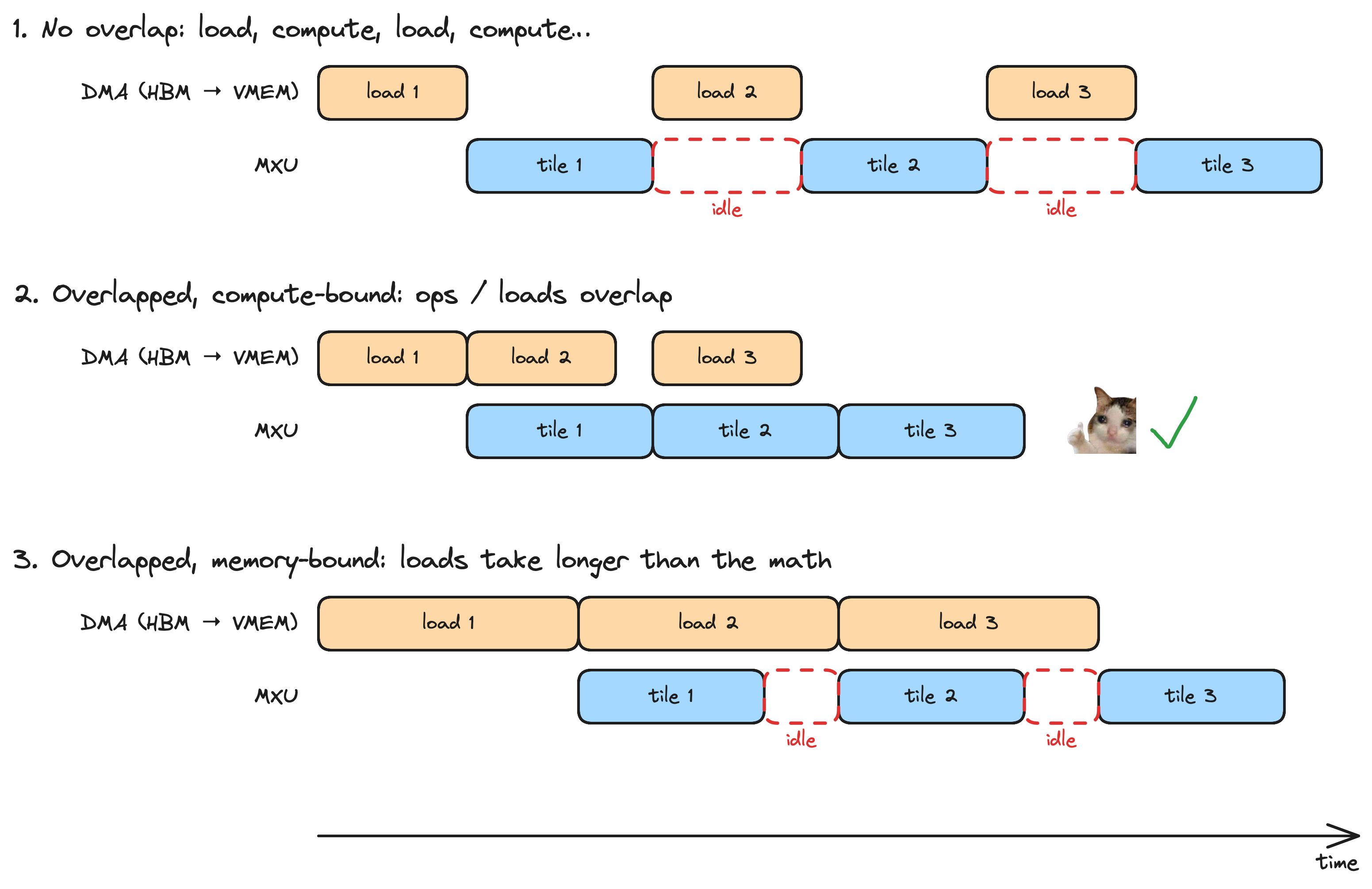
I listed these steps one after another, but in practice they overlap. While the MXU is working on one tile, the DMA engine is already copying the next one from HBM into VMEM, so the MXU doesn’t have to wait.
Here’s what that looks like over time, with and without overlap:
Compute-bound vs. memory-bound
An important part of thinking about TPU and GPU performance is considering what is slowing down the matmuls.
Essentially, every tile trip has two costs. There’s the time the MXU spends doing math, and the time the DMA engine spends moving data from HBM. Whichever one is slower is the bottleneck.
what does compute-bound / memory-bound mean?
Compute-bound means the data shows up faster than the MXU can use it, so the math is the bottleneck. Memory-bound means the MXU finishes a tile and then sits idle, waiting for the next one to arrive from HBM, so the memory is the bottleneck.
It is important to think about HBM bandwidth (on TPU7x, this is about 7.4 TB/s) here. In memory-bound workloads, it sets the ceiling on how fast the computation can run since the compute units can only work as fast as data arrives.
To figure out what type of “bound” you are, you compare two numbers:
what is arithmetic intensity?
The number of math operations (FLOPs) you do for every byte you pull from memory. A workload that does lots of math per byte is compute-bound, and one that does very little math per byte is memory-bound.
The chip has its own built-in ratio: its peak compute (for TPU7x, 2.3 PFLOPs/s) divided by its HBM bandwidth (for TPU7x, 7.4 TB/s). For TPU7x, that works out to roughly 300 FLOPs per byte. If your workload’s arithmetic intensity is above that ratio, you’re compute-bound. If it’s below, you’re memory-bound.
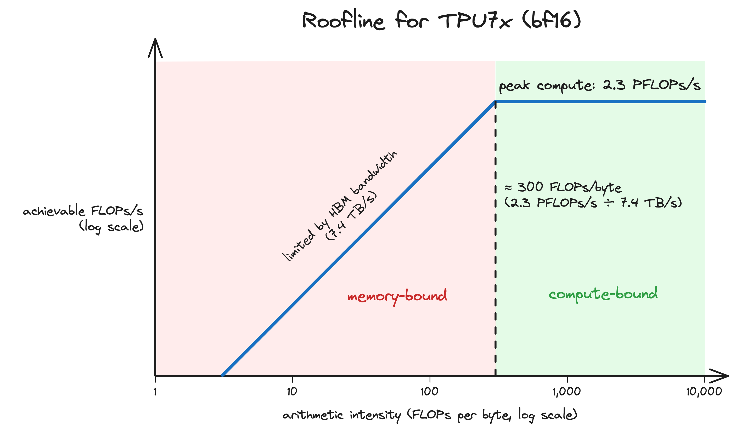
Generally, you want to be compute-bound because this means you are getting the full FLOPs you pay for.
TPUs are Cool
Long story short, TPUs are powerful matrix multipliers. I hope this blog post helped demystify them a bit, and encourage you to dig more into any parts that interest you. Some areas I plan to dig into next:
- Ragged Paged Attention
- Benchmarking Attention Kernels